Eccentric Computing
Implementation of a 16-bit One Instruction Set Computer (OISC)

One Instruction Set Computer (OISC) Overview
The goal of this project was to implement a Turing-complete One Instruction Set Computer (OISC) CPU using basic logic chips.
CISC (Complex Instruction Set Computer) CPUs of the 8-bit era had tens to hundreds of core instructions; current computer CPUs have thousands.
Many smartphones, printers, and other devices use RISC (Reduced Instruction Set Computer) processors with under 100 core instructions (which has processing and speed advantages).
That's why a OISC CPU with a single instruction is adorably ironic. Each instruction does not even have to be listed in the core program because, well, there's only one each could be :) Being Turing-complete means (apart from its physical resource limits) it can run any arbitrary program, like any other conventional CPU can.
Technical Goals
-
A OISC CPU based on the SUBLEQ instruction
-
Built on basic logic IC's (chips)
-
EEPROMs for state machine operation and complex logic lookup
-
1MHz CPU clock rate
-
128KiB Memory (64KiWords)
-
16-bit Data Bus
-
16-bit Address Bus
-
Hexagonal physical design with plug-in modules
-
8KiWord EEPROM (shadow copied to Address 0000 on boot)
-
Memory-Mapped Input/Output
-
A universal bus architecture (any compatible board can be plugged anywhere on the bus)
How it Works
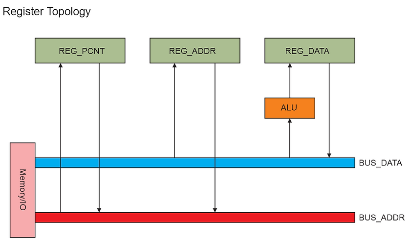
The CPU is built on a simple architecture that interconnects memory and three registers via two buses and a simple Arithmetic Logic Unit (ALU). The ALU is only required to add and subtract to perform its role in the SUBLEQ CPU. Note that there are no status registers needed. Also, as is described further in the programming section, there are no hardware registers (such as an accumulator) nor a stack pointer - these are implemented virtually by the assembler.
The design, once debugged, was produced on a 4-layer Surface Mount Technology (SMT) board, assembled and soldered by machine. (I only solder through-hole components, generally, which is why debugging on through-hole boards is preferred in my workflow.)
The CPU operation page has further technical detail on how the CPU works.
See the prototype page for details on the early design and testing of the CPU in a though-hole state.
OISC Firmware
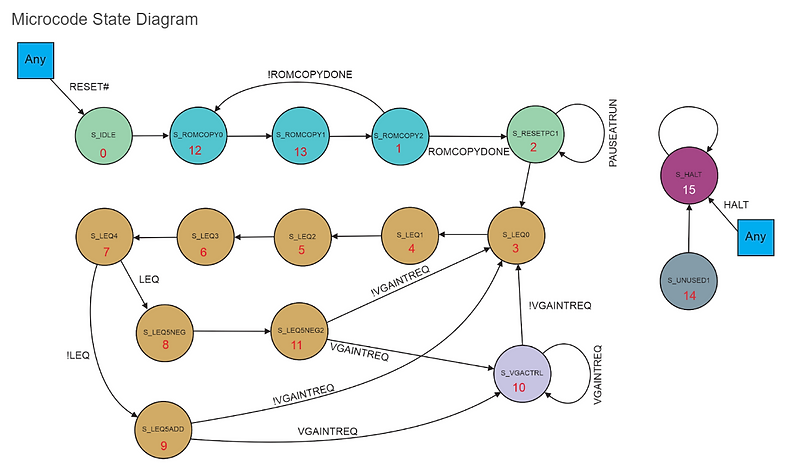
The OISC has three 64KiB EEPROMs containing its firmware, rather than using tens of Small Scale Integration (SSI) logic gate ICs. An additional advantage is that the firmware can be updated without hardware changes.
The first EEPROM contains static logic as a logic decoder. The memory image is generated by a custom-written C# program that takes as its input a high-level lookup table of logical highs, lows, and don't cares.
The remaining two EEPROMs form a state machine, which is generated from a high-level description and converted to EEPROM memory images with the custom C# program mentioned above. The state machine is responsible for performing all the sub-instructions that form the SUBLEQ instruction (e.g. memory and register transfers and ALU control) as well as copying the boot ROM (EEPROM) image to RAM to be executed.
All images are written to text files with CRC32 checksums, which are copied to an SD card for downloading into the EEPROMs. As I didn't have an EEPROM programmer, I designed one to plug into an Arduino Mega board. The Arduino reads the program off the SD card, programs the EEPROM, checks the CRC, and displays the result status via a series of LEDs.
There is another page that describes the above utilities in further detail.
Note that copying the program to the OISC is done in a similar manner, using a custom-built assembler to build the memory image (further details below).
Programming the OISC

Programming in SUBLEQ is pretty challenging, even though there is only a single instruction. Additionally, there are no status flags in the CPU to assist with branching, nor are there any general purpose hardware registers (or even an accumulator). Nor are there any instructions that could make use of these hardware features if they existed.
The SUBLEQ instruction subtracts the contents of one memory location from the next (stores it there) and then jumps to the address held in the next memory location if the result is less than or equal to zero. (If the result is positive, the next sequential instruction is processed.) Sometimes, regardless of the result of the subtraction, the next sequential instruction should be processed, which gives rise to the "?+1" notation in the above diagram.
The nature of the single SUBLEQ instruction means that special attention needs to be given when manipulating memory locations so that spurious partial results are not inadvertently stored.
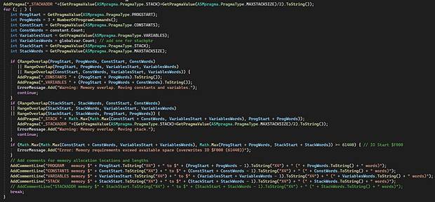
To make programming at least feasible (and a lot more fun) I created an assembler (in C#) that:
-
Included tens of different "synthetic" op-code mnemonics that recursively compiled into SUBLEQ commands. Commands were based on many of the common "6502-style" op-codes.
-
Allowed different addressing modes of the op-codes (e.g. Absolute, Immediate, Indirect, Implied, Absolute Indexed ...).
-
Had synthetic global registers (accumulator, X- and Y-registers).
-
Had synthetic stack pointers (and synthetic instructions to utilise them for function calls and returned values).
-
Allowed variables and constants.
-
Allowed entry in different mathematical bases (decimal, hex, and binary) and ASCII.
-
Included arrays and strings.
-
Allowed address labels for branching.
The assembler included an emulator, which allowed the compiled SUBLEQ code (with comments showing the original synthetic instructions) to be run on a PC, stepped through, and watches put on memory locations, the synthetic registers, and stack pointers.
The assembler software output memory image files (high-byte and low-byte) with checksum for transfer via an SD card to the EEPROM programmer to burn the "Boot ROM".
Click to find out more information about the OISC assembler, emulator and synthetic assembly language.
Clock and Power Module
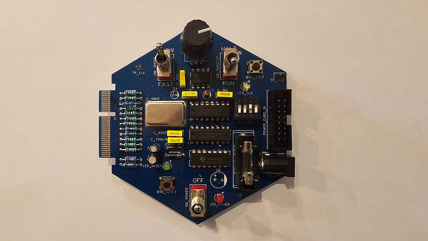
The Clock and Power module is a combined circuit that powers the bus while offering power protection mechanisms. It also elegantly provides several clocking modes for operation and debugging purposes.
Clock
-
The clock provides a fast mode and a slow mode, as well as a manual step-through mode.
-
The fast mode uses a 4MHz crystal oscillator with a divisor set by a 4-way DIP switch and down-counter IC. The approximate high-frequency clock runs from 133kHz to 2MHz, depending on the DIP switch settings.
-
The slow mode is based on a 555 timer, and adjusted with a potentiometer. Depending on the choice of fixed R/C components, the potentiometer allows for adjustment between approximately 2Hz and 1kHz. The variable adjustment circuitry introduces a non-linearity into the duty cycle, so to ensure it is at 50%, the output of the 555 IC is fed into a JK-flipflop (configured as a T-flipflop) to flip the clock output state on each rising edge of the 555 output.
-
The manual step-through mode uses a PCB-mounted push-button switch with debounce circuitry (low pass filter).
Power
-
Provides a protected 5V input to the bus, with some capacitive filtering.
-
Input to the modules is from either Eurorack power supply or a 5V DC "plug-pack" supply.
-
A reset pulse is generated for the bus upon power-up (or via the embedded reset button).
-
Protection of overvoltage, or reversed polarity, is provided via a reverse-biased diode to GND (not in series to avoid unnecessary voltage drop) and fuse, along with a 5.6V zener diode.
Take a Closer Look

RAM Module
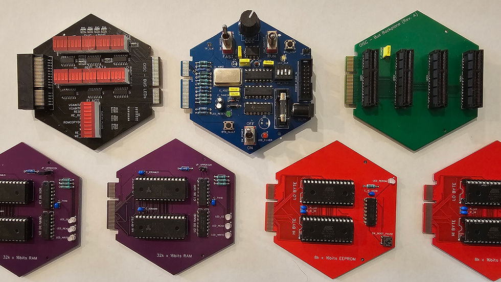
Each RAM module contains 32KiWords of static RAM. There is a jumper to indicate whether the board is the low 32Ki or high 32Ki, and onboard logic to enable the RAM ICs depending on the address and jumper. LEDs give a visual indication of board selection, and read and write line statuses.
ROM (EEPROM) Module
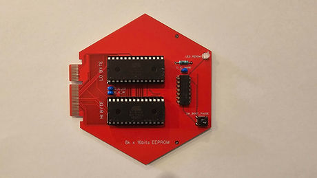
The ROM board is used to store the program to be run by the OISC. It is very similar to the RAM module, except EEPROM chips are used, so no write logic is required. There is no jumper as the address range is always the lowest 8KiWords.
A pushbutton is provided that pauses the CPU when the ROM copy is completed and before execution begins. This allows for "instant" copying of the program at high speed, and then the clock can be put into slow- or step-mode before the button is released.
Bus and Status Indicators Module
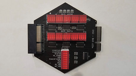
The Indicator module uses LED bar graph modules to display the status of the Data and Address values on the bus, along with the most important control signals. Buffer ICs were used to drive the LEDs, reducing current loading on the bus.
I/O Module (Prototype)
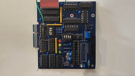
This prototype Input/Output (I/O) board is to test memory-mapped I/O controlled by the OISC's main bus and without special instructions. Some functionality includes:
-
DIP switch board selector for up to 16 boards
-
8 bit latched I/O with 8 bit board status on high data byte
-
LED bargraph and status indicator outputs
-
Inputs from switches and pushbuttons
-
Header for 16x2 LCD
-
Arduino socket to interface UART, Analog I/O, keyboard, VGA display
-
Headers for SD card I/O and SPI interface
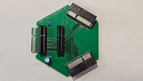
Bus Expander Module
The Bus Expander simply connects four additional ports to a horizontal one. The individual ports on the bus are not addressed, so they can be expanded until loading or capacitance becomes a problem.

CPU 4-Layer PCB Design
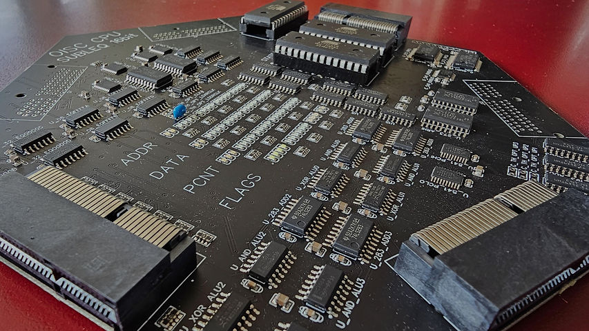
The main CPU board was mostly auto-routed with four layers using Freerouting. Issues with the hexagonal design meant a significant amount of hand-routing was required around the edges.
OISC in Action

The video shows the CPU running at a medium clock rate. The program counter (PCNT) initially counts up (and is used on the address bus) as the boot image is copied into RAM. The program runs (modifying the DATA and ADDR registers as it does so) and the program ends when the program jumps to address FFFF.